How can a doctor tell what sort of disease you have? All diseases – from cancer to the common cold – produce special chemicals called antigens which give away what they are. The problem is that often there are only very small amounts of these chemicals in your blood, which makes it hard for doctors to find them. We need special equipment which are sensitive to these chemicals – and that’s where nanotechnology can help.
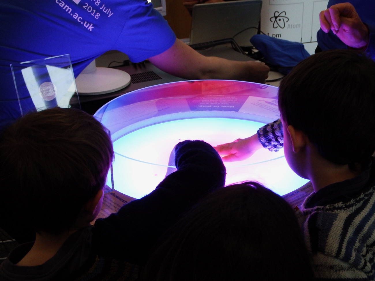
We can find diseases using sensors made out of a material called graphene. Graphene is like the membrane you can see here, but much, much smaller. Graphene is made from graphite (the stuff that pencils leads are made out of). We use graphene because it’s incredibly thin – a sheet of graphene is made from a single layer of carbon atoms. The thin graphene surface is extremely sensitive to anything touching it, like a very thin and delicate membrane. We can add antibodies to the graphene which stick to the antigens, the way the magnetic balls stick to membrane. Every antigen has a unique antibody that it can bind to – they fit together like a key in a lock.
 When the balls stick to the membrane here, it vibrates less. In a similar way, when antigens stick to the antibodies on the graphene surface, they change the way the surface reflects light and the way that electricity flows through it. 2D materials like graphene are important because the graphene surface is very sensitive to anything stuck it, so it can find very small amount of antigens. With a graphene sensor like this, we may soon be able to use a small sample of blood to find out what diseases you have.
Articles on this Subject:
2D Material Growth
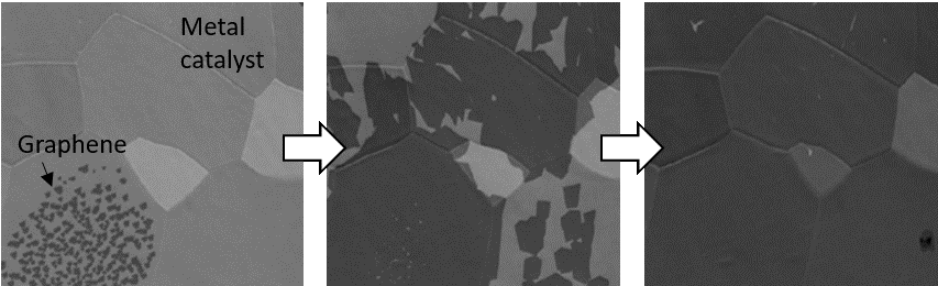
2D materials such as graphene and hexagonal boron nitride are only one atom thick. However, we can still directly observe them and even watch how they grow on metal catalysts at temperatures as high as 1000 degrees Celsius! Armed with this information, we can understand how to grow these materials better and improve their quality for applications ranging from electronics to bio-sensors.
This is possible using techniques such as scanning electron microscopy, which uses an extremely powerful microscope to directly image things on the nano-scale, and X-ray photoemission spectroscopy which gives us information about the chemical processes that occur.
Check out the links below to find out more about through work from the Hofmann group.
Journal References:
S. Weatherup et al., In Situ Graphene Growth Dynamics of Polycrystalline Catalyst Foils, Nano Lett., 2016, 16(10), 6196-6206
http://www-g.eng.cam.ac.uk/hofmann/publications/pdfs/152.pdf
R. Kidambi et al., In Situ Observations during Chemical Vapour Deposition of Hexagonal Boron Nitride on Polycrystalline Copper, Chem. Mater., 2014, 26, 6380-6392
http://www-g.eng.cam.ac.uk/hofmann/publications/pdfs/117.pdf
2D Material Sensors
From understanding how they grow and what their properties are, we can then use this information to make useful sensors from them. Below are a couple of examples of work that has already been done.
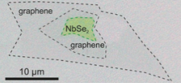
Individually, 2D materials have novel properties. They can also be combined into what are known as van der Waals heterostructures, which are layered “sandwiches” of materials. In the paper linked below, the authors create a heterostructure from graphene and NbSe2, combining the mechanical strength of graphene with high conductivity of NbSe2 to make a high quality factor mechanical resonator. This is a sensor which works by vibration just like in our exhibit. They show that the electrical resistivity is low and the frequency may be tuned and suggest this is a good proof of principle when sensing force in ultra-small and lightweight devices.
Journal Reference: M. Will et al, High Quality Factor Graphene-Based Two-Dimensional Heterostructure Mechanical Resonator, Nano Lett., 2017, 17, 5950 https://pubs.acs.org/doi/pdf/10.1021/acs.nanolett.7b01845
The second example is a device made out of a material called silicon nitride. Similar to the device above, it is a resonator, so detects mass through changes in vibrations. The device surface is made sensitive specifically to a mouse protein by attaching the antibody to the surface. Protein antibodies are used as “key and lock”: only the protein can attach to the antibody. This makes the sensor very specific. When any protein passes by the sensor, the antibody will bind to it. This sensor shows that it has found some protein by changing colour and by mass changes, which change the resonant frequency.
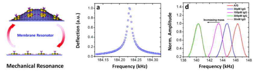
Journal Reference: A. Zhu et al., Optoelectromechanical Multimodal Biosensor with Graphene Active Region, Nano Lett., 2014, 14, 5641
https://pubs.acs.org/doi/pdf/10.1021/nl502279c
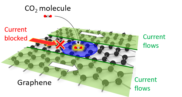
The ultimate gas sensor would be so sensitive that it would be able to detect individual molecules one by one. This is no trivial feat as the signature of a single molecule, whether it be its size, mass or electric charge, are incredibly small and difficult to detect! Yet in this paper, the authors use graphene to do exactly this and detect individual CO2 molecules.
In this work, an electrical current is passed through the graphene. As each CO2 molecule attaches to the graphene surface, it adds to the graphene’s electrical resistance by a fixed amount by scattering the electrons in the current, allowing individual molecules to be measured. This is only possible because of graphene’s 2-dimensional nature, making it extremely sensitive to anything that binds to it.
Journal Reference: J. Sun et al., Room Temperature Detection of Individual Molecular Physisorption using Suspended Bilayer Graphene, Science Advances, 2016, 2(4) http://advances.sciencemag.org/content/2/4/e1501518/tab-pdf
Research Horizons- http://www.cam.ac.uk/people/stephan-hofmann
Groups working in this field:
 The Hofmann group explores novel materials, metrology and device architectures. A particular focus thereby lies on nanomaterials and the use of in-situ metrology to probe the fundamental mechanisms that govern their growth and functionality. Understanding matter on the nano-scale has huge technological potential in energy conversion and storage, information/communication and environmental technologies.
Sensing in Flatland